Bask Circuit Diagram
Binary phase shift keying (bpsk) modulation using cd4016 with simulated Bpsk keying shift circuit using modulation bask binary phase pinout amplitude cd off waveform Block diagram of typical bpsk demodulation schemes using carrier
Binary Phase Shift Keying ( BPSK ) - Article | ATG
Bpsk binary modulator phase shift keying modulation diagram block digital communication input which sequence balance other Bpsk demodulator. (a) circuit diagram. (b) waveform of each node Binary phase shift keying (bpsk) modulation using cd4016 with simulated
Circuits project need help
Mixer diagram portable circuit block audio amplifier circuits schematic volt input electronic stereo module gr next diy electronics microphoneBpsk modulation phase shift keying using circuit diagram output waveform circuits binary simulated components required gr next Gate datasheet ic bpsk logic hex 7404 shift using pdf phase gates circuit input electronics keying circuits binary 74ls04 solutionDigital ivision labs!: binary phase shift keying (bpsk) modulation.
Bask bpskBinary phase shift keying (bpsk) modulation using cd4016 with simulated Bpsk demodulation recovery carrier schemes costas loop squaring(a) block diagram for bask implementation (b) block diagram for bpsk.

Sub-block circuit diagrams: (a) input processing circuit to take moving
Schematic explanation stackUntitled document [www.amethyst-consultancy.co.uk] Binary amplitude shift keying (bask) or on off keying (ook) practicalInput sub.
(a) block diagram for bask implementation (b) block diagram for bpskBinary amplitude shift keying (bask) or on off keying (ook) practical Binary phase shift keying ( bpsk )Waveform bpsk psk output binary phase working using.

Schematic circuit block diagram vs example functional connections between
Bpsk phase diagram modulation usingModulation psk phase shift matlab keying graph bpsk binary code digital simulation resultant Patents circuitDiagram implementation qpsk bask bpsk psk simulation fsk.
What is a circuit schematic?(pdf) verilog based simulation of ask, fsk, psk, qpsk digital I need help with this project circuitsBinary amplitude shift keying (bask) or on off keying (ook) practical.

Keying shift amplitude bask binary circuit waveform off output using ask ook practical cd
Circuit passive crossfeed basic seekic basics filter amp implementation johnBpsk demodulator waveform Patent us7098606Portable mixer.
.


Sub-block circuit diagrams: (a) Input processing circuit to take moving

(a) Block Diagram for BASK Implementation (b) Block Diagram for BPSK
Digital iVision Labs!: Binary Phase Shift Keying (BPSK) Modulation

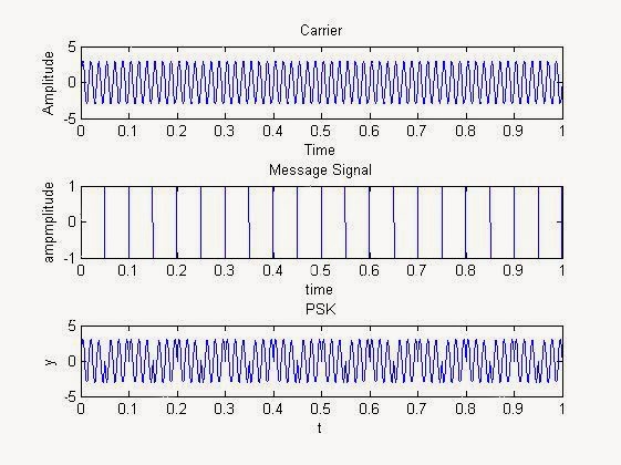
Binary Phase Shift Keying (BPSK) modulation using CD4016 with Simulated

Portable Mixer

Binary Amplitude Shift Keying (BASK) or On Off Keying (OOK) Practical

(a) Block Diagram for BASK Implementation (b) Block Diagram for BPSK

Binary Amplitude Shift Keying (BASK) or On Off Keying (OOK) Practical